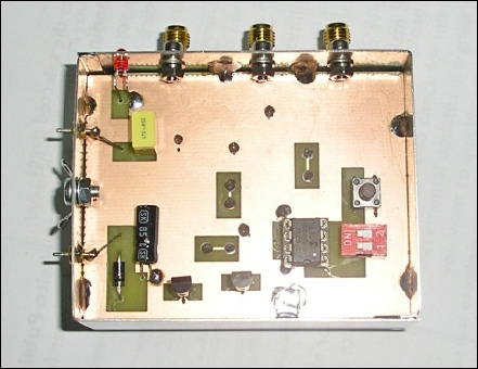

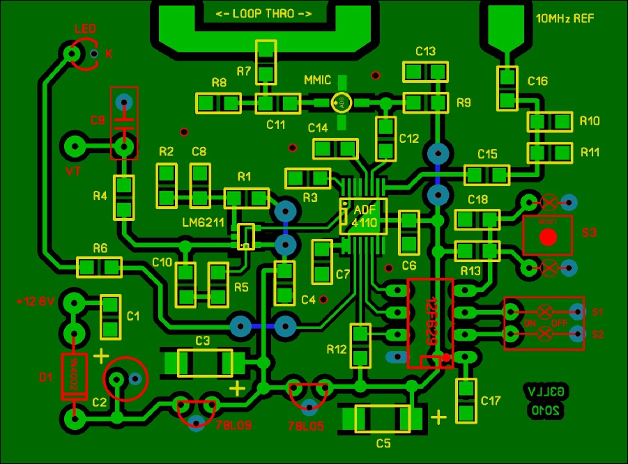
The double-sided PCB layout seen from above with the YELLOW SMD and GREEN track layers underneath. The RED through-hole components and BLUE pads/links are on top together with five small RED circles indicating riveted vias. Pin-8 of the 12F629 is soldered on both sides of the board.
A viewer and print utility for this layout is available on the “Software” page.

Home : Schematic : Description : Software